- 当前位置:
- >
- 首页
- >
- 展会资讯
- >
- 半导体行业
- >
- 报名参加光刻与3DIC培训 成就未来更好的自己
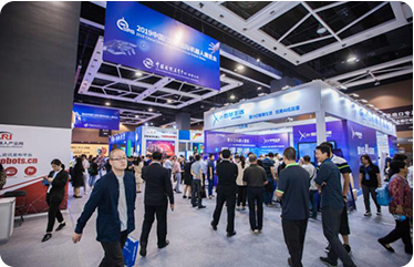
半导体行业资讯更多
报名参加光刻与3DIC培训 成就未来更好的自己
| 分享: |
| Photolithography and Related Technologies and Process Standards光刻的相关技术、工艺与标准Date: 13:30-15:00 on March 25, 2025Meeting Room: 5B+5C | |
Speaker:Prof. Qiang WuProfessor of the School of Microelectronics of Fudan University | |
| Abstract:This tutorial will provide the audience with an overall introduction to the photolithography process, related equipment, material, and process standards and future outlook. For the process and related equipment and material, I will present the following: a brief history of optical science and technology, the basic imaging theory, process window parameters and optimization, Source-Mask co-Optimization (SMO), exposure tools, photoresists, photomasks, computational lithography algorithms, the optical proximity correction (OPC), and the EUV lithography. For the part of the process standards, I will discusson the standards for linewdith uniformity, process window parameters, and resolution limit of EUV. Finally, an outlook will be provided from the author's perspective.Biography:Dr. Qiang Wu is a Professor at Fudan University. He graduated from Yale University with a Ph.D. degree in 1999. Then he worked for several companies as a photo engineers and managers. His research interests includes lithography process, equipment/material development, computational lithography, etc. He has published 83 papers and 112 patents. |
| Advanced Package and 3DIC (Chiplets and HBM)先进封装与3DIC(Chiplets与HBM)Date: 15:30-17:00 on March 25, 2025Meeting Room: 5B+5C | |
| Speaker: Dr. Guorong LiVice President, Beijing NAURA Technology Group Co., Ltd. | |
| Abstract:Currently, as Moore's Law progresses towards its limit, advanced packaging technologies such as TSV (Through Silicon Via) as a representative of 2.5D & 3D packaging have become an important way for chip higher integration. Etching process is the key and difficult point in the entire advanced packaging technology. The main difficulties are the morphology control of high aspect ratio (AR greater than 30:1) etching, such as sidewall roughness, lateral side etch control of the stopper layer, and edge inclination control. The other difficult point is the etching technology for the backside leakage of TSV after Cu filling. It involves the challenges of particle pollution control, cost control, and mass production stability. After years of technological exploration and development, NAURA has already achieved stable mass production of TSV process, backside Cu leakage process, and other multi-step etching processes for several customers.Biography:Dr. Li Guorong graduated from the Electronics and Information major at Peking University. He is currently the Vice president of Etch I BU and in charge of the 12-inch Etching Product Line at NAURA Co., Ltd., with over ten years of experience in the semiconductor etching equipment field. He is an expert in developing front-end and packaging process and equipment solutions, and has rich experience in the development and mass production of ICP and CCP etching equipment. | |
| Speaker: Dr. Xia JiangChief Scientist, JCET SEMICONDUCTOR INTEGRATION (SHAOXING)CO., LTD. | |
| Abstract:In the post-Moore era, advanced packaging technologies represented by 2.5D/3D are gradually becoming a new breakthrough in the semiconductor industry. The report details the history of the development of advanced packaging, introduces and interprets representative advanced packaging technologies and processes of the present day, especially the high-bandwidth memory (HBM) die integration packaging structure based on 3D stacking. It also elaborates on the applications and development trends of HBM based on 3D packaging.Biography:Xia Jiang, Ph.D., Chief Scientist at JCET SEMICONDUCTOR INTEGRATION (SHAOXING)CO.,LTD. He has been working on the R&D and manufacturing of 2.5D/3D wafer-level fan-out advanced packaging technologies. Focusing on high-performance chip integration such as HBM, GPU, CPU, APU, he has lead multiple development projects on ultra-high-speed, low-latency fused interconnect chiplet packaging. He is the author and co-author of multiple research papers, book, and invention patents. |
SEMI U TUTORIAL
Date & Venue
Tuesday, March 25, 2025
Shanghai International Convention Center上海国际会议中心上海浦东滨江大道2727号No.2727 Riverside Avenue Pudong, Shanghai 200120, China
SEMI U TUTORIAL
Registration (RMB)
CSTIC 2025 Registration Price (RMB)
● SEMI和IEEE-EDS联合主办,中国规模最大、最全面的年度半导体技术会议。● 超百位世界领先的行业及学术专家汇聚一堂,内容涵盖IC设计、半导体器件与集成、纳米薄膜、光刻、蚀刻、CMP、封装测试、AI与IC制造等各项前沿技术。● 大会主题演讲、十大分会场、圆桌论坛、培训课程线下齐开,超600场专业演讲与海报将在现场和网上展示。现场与行业领袖、技术和学术专家面对面交流沟通,4周的网络会议延续与讲师的问答。识别下方二维码或点击文末“阅读原文”立即注册参会,享受早鸟优惠。
Conference Questions: April Peng, SEMI ChinaEmail: Cheryl Qiu, SEMI ChinaTel: 86.21.6027.8552Email: cheryl.Sponsorship Contact: Xianbo Sun, SEMI ChinaTel: 86.21.6027.8569Email:
(扫码免费自助发产品)
点击关注SEMI
SEMI产业投资平台
PSO
阅读原文
展会咨询
相关半导体行业展会

微信小程序

扫码进入小程序
微信公众号

扫码进入公众号


- 客服

- 电话
服务热线

- 扫一扫
 |
 |
 |
 |
世展网公众号 |
微信小程序 |
销售客服 |
门票客服 |

- TOP